3D COMPUTER CHIPS
A 3D chip is an integrated circuit that consists of multiple Three dimensional devices that perform various functions, such as image processing,and neural network which can be analog or Digital in some cases both. It addresses some of the challenges of designing high-end chips with smaller footprints or size.
The increasing number of transistors which is due to the size of the chip been smaller but powerful has resulted in the wires connecting these components becoming thinner and closer together, which can cause overheating and signal delays as the speed of the clock to the central processing unit is limited.
In April 2007, a new generation of 3D chips was announced, which were made by a collaboration between IBM and the RPCI Institute. The chips were made using a technique known as wafer bonding where 3D chips are placed upon one another. IBM's approach works by placing a processor on the bottom of a stack, while other components are layered on top.
This technique allows engineers to place a monitor or other components on top of the processor, which results in a thousand-fold decrease of connector length.
Through-silicon vias allows multiple components to be stacked vertically, which results in faster and smaller CPUs. IBM also introduced a new method of manufacturing that allows the same components to be placed on top of each other.
Through-silicon vias help minimize heat dissipation through the stack and improve the power-efficiency of silicon-germanium based products by about 40% making the battery last longer
IBM's 3D-based memory-on-processor technology is already being used in mobile devices and will be available in 2009 for servers and supercomputers. In February 2007, Intel also announced that it could perform calculations with teraflop capabilities.
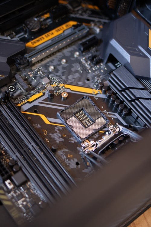
A microchip is built by layers on a silicon wafer. The layers are made by a process known as photolithography, which uses light and chemicals. This process coats a surface using a light-sensitive material, which is known as photoresist. It hardens the areas exposed to ultraviolet light.
The processes used to build a microchip begin with the overlaying of a thin layer of metal, which is usually aluminum. The resulting conducting pathways are then left to be used. Jack Kilby and Robert Noyce were the inventors of microchip technology. Their achievements were acknowledged by the US Patent Office in 1959.
TYPES OF 3D COMPUTER CHIP
1 3D packaging
3D packaging refers to the process of implementing 3D integration schemes through the use of traditional methods such as wire bonding and flip chip to get a vertical stack. 3D packaging can be further broken into two namely 3D SiP (system in package) and 3D water level package (3D WLP) with Stacked memory die connected to wire bonds and package on package (POoP) configuration.
PoP is a type of thin film package that is used for vertically integrating various technologies such as 3D WLP. It involves the use of various processes such as reflow layers (RDL) and wafer bumping.
2 SD ICs:
SD ICs can be divided into SIC (3D Stacked ICs) and Monolithic 3D ICs.
3D STACKED ICs (SIC)
The 3D stacked ICs are type of chips that uses TSV interconnects and are typically used for mobile devices. Due to the increasing number of components in the digital electronics market, the need for a higher density memory solution has been suggested.
This issue can be solved through the use of multiple die stacking techniques. In August 2014, Samsung started to produce 64 GB of 3D TSV modules for servers.
MONOLITHIC 3D ICs
The Monolithic 3D ICs uses the gave process to get 3D interconnects at the local level of the wiring hierarchy. first examples of a monolithic 3D IC approach were shown in Samsung's 3D V-NAND devices.
In Monolithic 3D ICs, the layers are built on a single substrate, and then sliced into 3D modules. This eliminates the need for alignment, bonding, and through-silicon vias.
The first step in 3D TSV production involves a high temperature transfer process, which is known as layer transfer.
After that, the layers are deposited using an ion-cut technique. Using low temperature bond and cleave techniques, multiple thin silicon layers can be created that are defect-free.
ADVANTAGES
1 Moore's law has allowed more functionality to fit into a small space. 3D stacking simplifies the process by creating multiple dies that are smaller than a single chip and gives rise to a tiny but powerful devices.
2 circuits can be built with various processes and different types of wafers. This means that component that aren't s can be assembled in a single 3D IC.
3 The average length of wires used for 3D interconnect is typically reduced. However, due to the high capacitance of 3D wires, circuit delay may not improve.
4 A signal on-chip that consumes less power can reduce its overall consumption by up to 100 times. Shorter wires can also reduce the amount of parasitic capacitance.
5 The vertical dimension of 3D integration allows designers to add more connectivity and new design possibilities. However, it can also create security issues due to the stacked structure.
6 3D integration also allows system monitor-like features to be added in. This allows system administrators to monitor and protect the entire electronic system from unauthorized access.
7 3D integration allows designers to build wide bandwidth buses between various functional blocks. For example, a processor+memory 3D stack is commonly used. It allows a bus to be wider than the 256 bits required for mainstream applications.
LIMITATIONS
1 Due to the complexity of 3D technology, its commercialization has been identified as a challenge. However, the work is already done to address this. Although 3D technology is new and relatively complex, the cost of manufacturing is easily identified when broken down into its various activities.
The cost drivers are identified and can be optimized to reduce the cost of production. Doing so can help avoid adding additional steps and improving the defect density.
2 Heat build up within a stack is inevitable. However, it can be managed through the use of various strategies and tools.
3 TSV-introduced overhead gates and impact floorplans are larger than traditional gates and require more landing pads and keep-out zones to decrease their overall area footprint.
Depending on the design choice, TSVs can be made before metallization or after metallization. These can occupy the device layer and prevent them from accessing the chip.
In addition, they occupy the metal layers of the device, which can result in routing obstacles and placement issues. The overall yield can vary depending on the type of granularities and gate-level partitioning. It can also decrease for finer granularities.
Even with the tight integration between the active layers, some sections of a 3D IC can still require more than one layer of interconnect. Due to the massive overhead associated with TSVs, they cannot be independently tested.
4 There are little or few standards for 3D IC design, packaging, and manufacturing. Also, there are many options for integrating TSVs, such as via-last, through-middle, interposers, and direct bonding. Unfortunately, many 3D IC suppliers are still unclear about who owns the 3D IC parts and assembly.
REFERENCES
https://whatis.techtarget.com/definition/3-D-chip-3D-chip?amp=1
https://news.mit.edu/2017/new-3-d-chip-combines-computing-and-data-storage-0705
https://infinigeek.com/when-are-3d-chips-going-to-arrive-newsflash-theyre-already-here/?amp=1
https://www.livescience.com/52207-faster-3d-computer-chip.html
Congratulations @tough! You have completed the following achievement on the Hive blockchain and have been rewarded with new badge(s):
Your next target is to reach 500 upvotes.
Your next target is to reach 50 replies.
You can view your badges on your board and compare yourself to others in the Ranking
If you no longer want to receive notifications, reply to this comment with the word
STOPCheck out the last post from @hivebuzz:
Support the HiveBuzz project. Vote for our proposal!
This amazing technology.Will this technology have an impact on smartphones, or is it only used in other types of devices? What can we expect in the way of breakthroughs if this technology gets implemented in the smartphone industry?
Thank you for this well written and insightful article.