Informatika | Junctions : diodes and transitors
Hello everyone,
[FRENCH] Pour les français, cet article est la traduction anglaise de ce post, mes posts à caractères scientifiques sortant toujours avant leur traductions anglaises, vous pouvez surement d'ores et déjà lire le prochain article en langue française.
In the last post, (a long time ago now) of Informatika we were interested in the basics of modern electronics, namely semiconductors. Explaining briefly the principle of operation of semiconductors and their design. We came to define 2 main types of semiconductors, the positively doped semiconductors, of P type and presenting holes, and the negatively doped semiconductors, of N type presenting electrons. We are now going to focus on the relationship between these materials and their applications in electronics.
Junctions
We have seen the principle of doping semiconductors. Let's now focus on the junction principle which is the fundamental principle used for the operation of diodes.
A junction corresponds to the joining of two semiconductors doped differently, we call these binary junctions P-N junctions. It is equivalent to N-P since it would be enough to return the structure in this case, the P-P or N-N junctions do not exist since they do not present any particularity.
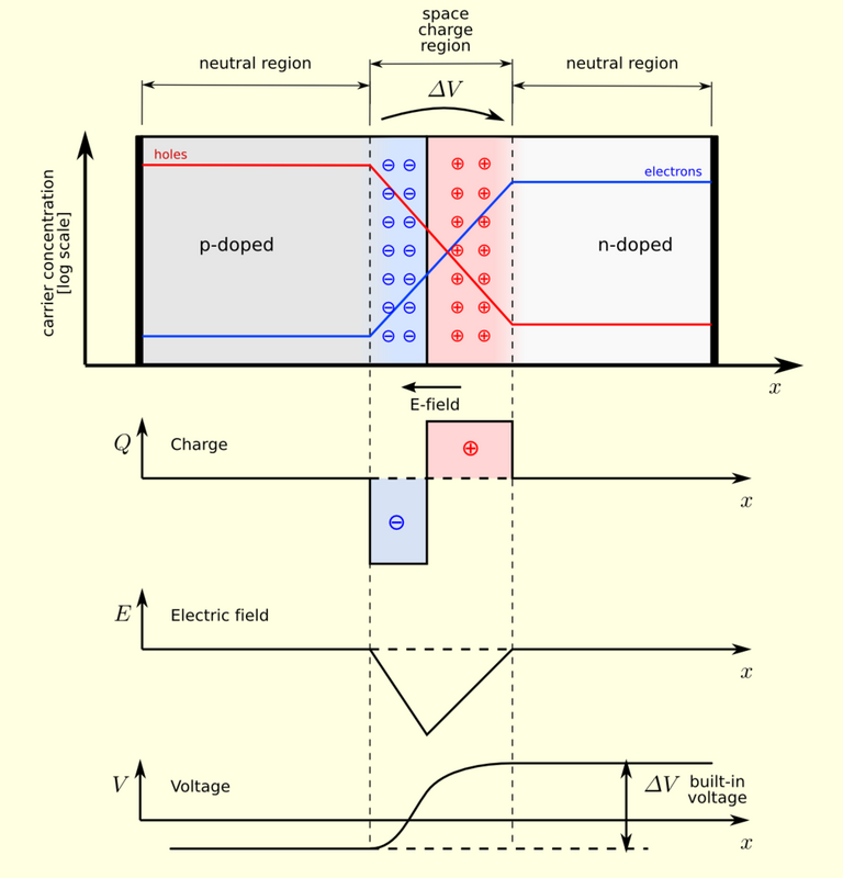 Space charge region [Wikimedia CC BY-SA 3.0]
 ![[Wikimedia CC BY-SA 3.0]](https://commons.wikimedia.org/wiki/File:Pn-junction-equilibrium-graphs.png)
The diode
Everyone who has done a minimum of electronics knows the principle of operation of a diode, it lets the current pass in one direction and blocks it in the other (or at least strongly enough for it to be negligible). Well, this is because a diode is simply a P-N junction.
Connected in the so-called indirect or blocking direction, that is to say by applying a negative voltage on the P side and positive on the N side, the electrons and holes are attracted to the nearest poles, (see diagram above). The electrons are attracted to the Cathode (N side often noted K) while the holes are attracted to the Anode (P side often noted A) enlarging the depletion region and thus preventing the flow of current. Until a phenomenon that I will not deal with here for reasons of simplification called avalanche phenomenon, I will leave a link to more information at the bottom of the post for the more curious.
Now, when we connect a diode in the forward direction, with a voltage higher than the junction potential, the electrons "injected" on the cathode side cross the depletion zone to then fill the holes in the P region or join and continue in the electrical circuit to the power supply. Thus the current flows through the diode.

Symbol of a diode Public domain vectors
The principle of LEDs, light-emitting diodes
In the life of all currently are present LEDs. You will have understood by their name, LEDs are diodes, emitting light. When the diode is passing and an electron comes to fill a hole its energy state changes from a free state to a bound state, of lower energy. A photon is thus created to emit this energy in the form of light. And the light is !
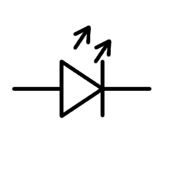
Symbol of an LED Wikimedia GNU Free documentation
Bipolar junction transistor
Another range of systems derived from the principle of semiconductor junctions is the family of transistors. Indeed, most transistors work thanks to semiconductor junctions. In particular the transistors we will focus on here: Bipolar junction transistor
The bipolar junction transistors, as their name does not indicate it at all are electric tripoles. It has 3 poles, B, E and C respectively the Base, the Emitter and the Collector.
There are 2 types of bipolar transistors from design: NPN and PNP transistors which as you will have understood are composed respectively of a NP junction put aside to a PN junction and a PN junction put aside to a NP junction.
The two types of transistors are quite similar, what differs is the direction of the currents and voltages of the two tripoles.
Transistor PNP symbol Wikimedia GNU Free Documentation
Transistor NPN symbol Wikimedia GNU Free Documentation
Operation of BJT
We are going to focus here on the operating principle of NPN type transistors because they are the most common, and if you have understood the operating principle of diodes and junctions you should easily understand the operating principle of PNP transistors.
In the case of an NPN transistor, each pole of the transistor is connected to a different doped region: the emitter to an N region that we will call N_e, the base to the positively doped region and the collector to the second N region that we will call N_c.
The emitter is polarized by a voltage lower than that of the base, we find the operation of a diode at the junction N_e/B and the current flows from the emitter to the P region.
As for the collector, it is inversely polarized, the voltage at the collector is higher than that of the base and the electrons diffused from the N_e area are therefore seen in the charge area of the P/N_c junction, all the current therefore flows from the emitter to the collector.
In addition, the pole of the base acts by varying the transmitted current exponentially relative to the potential difference between the base and the collector. The higher the voltage between these terminals, the higher the current transmitted to the collector. If the voltage at the terminals is zero then the diodes induced in the transistor are blocking and no current flows.
There are other models of transistor working thanks to the principle of semiconductor junctions but their operation is a little more complex and uses complex concepts to popularize. This is why I preferred to present only BJT. The field effect transistors, much more widespread nowadays are an example of transistor based on semiconductor junctions.
I still don't understand very well, please explain very simply
When two differently doped semiconductors are joined together, a region is formed where free electrons and holes recombine. This formation has the effect of modifying the principle of conductivity of these materials allowing to act as a valve in plumbing and to allow the flow only in one direction. The material is thus oriented (polarized) which implies a direction of the flowing current and a blocking direction.
This system composed of two semiconductors is what we call a diode.
When another semi conductor is bonded to a diode and under certain conditions, a transistor is created. A transistor is a system with 3 connections that allow to control the intensity of the current flowing through this dipole, the base, the emitter and the collector. To keep the analogy with plumbing, it is as if we had a portion of piping connecting the emitter to the collector in which there is a valve controlled by another pipe coming from the base. The greater the water pressure from the base, the greater the flow rate from the transmitter to the manifold.
Sources et ressources
I'm french so the resources I used to write this post are mainly french but I have other resources in english or that don't need to know how to speak french to be understood.
First here are courses coming from engineering schools freely available and having allowed me to approach these principles with a pedagogical vision, they are much more complete than this article and will surely allow you to go into more detail [FRENCH].
Here is a theoretical study of the electric field in a depletion zone, (most of it is written in french but mathematics and physics equation can be understood worldwide I think (I know that div and grad operator are not in use elsewhere than in France so : div and grad are nabla operator, div is for a Vector field as grad is for a scalar field)
Wikipedia - Approche théorique des jonctions PN
The ISMIN course also deals with the operation of diodes, I also used wikipedia articles.
Principle of operation of transistors, if you want to go into more detail
Wikipedia - Bipolar junction transistor
Field-effect transistor