CONDENSED MATTER PHYSICS: The Transistor, Semiconductor Lasers, and Superconductivity.
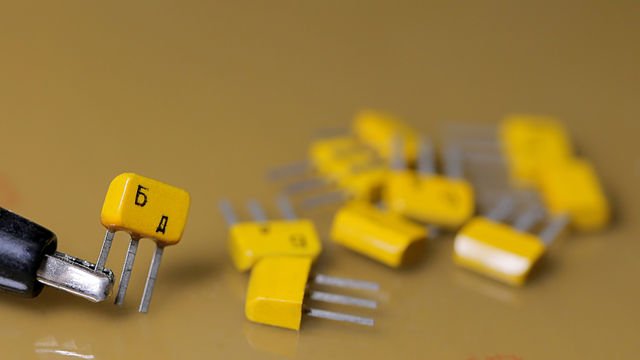
The transistor was invented in 1951 by John Bardeen, Walter Brattain, and William Shockley, at the Bell Research Laboratories in the USA; It is used very widely as a controllable switch.
The pnp transistor consists of a thin layer of n-type material sandwiched between two thicker regions of p-type material. The transistor turns on and controls a large current through one of a pair of pn junctions (see the sub-topic below) by passing a small current through the other. Transistors are particularly suited for controlling the on-off binary logic used in computers. They are available as discrete circuit components or as parts of integrated circuits.
The pn junction
A pn junction consists of a piece of p-type semiconductor joined to a piece of n-type semiconductor. The lattice of atoms in which the p-type and n-type impurities are inserted is often the same material. Excess holes exist in the p-type material and extra electrons in the n-type material and it is these which can carry current.
Very close to the junction, the holes and electrons cancel each other out, so that there are very few free carriers here. This region is called the depletion layer. Because there is now a shortage of holes on the p side of the junction, it is as if there is a negative charge there relative to the rest of the material, and the shortage of electrons on the n side makes this a positively charged region. This gives rise to a contact potential maintained by the distribution of holes and electrons; there are no charge carriers, so there is no current.
THE JUNCTION DIODE
Let’s apply a reverse bias to the pn junction. This means that we apply a voltage difference across the junction with a positive voltage going to the n-type side and a negative voltage to the p-type side. This increases the contact potential and attracts even more free carriers (both holes and electrons) away from the contact region.
If we apply the voltage difference the other way round, in forward bias, the applied potential difference will cancel the contact potential. The depletion layer is narrowed and then removed and the pn junction conducts normally. Hence the junction passes current in forward bias but not reverse bias and can be used as a junction diode for rectification, meaning that current is allowed to pass in one direction only.
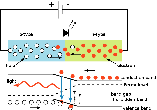
THE LIGHT-EMITTING DIODE
A light-emitting diode (LED) is made from a junction of two semiconductors, gallium phosphide, and gallium arsenide. A current passes one way only, as in an ordinary junction diode, but when current passes through the junction light is emitted as electrons drop between energy levels.
Red, yellow and green LEDs have been in use for some time, but more recently blue LEDs have become practicable. For blue light ( λ = 450 nm), a forward voltage drop across the junction of 2.8 V is needed. Gallium nitride (GaN) LEDs have been developed with forward voltages of 3.4 eV (λ = 360 nm) and aluminium nitride (AlN) LEDs with ultraviolet outputs (6.2 eV).
LEDs can now be made as bright as a 500 W traffic light while using just one-tenth of the energy. They have taken over from battery-thirsty filament bulbs in, for example, bicycle lamps; and, because they respond (light up) more quickly, they are ideally suitable for car stoplights. Ultraviolet LEDs could also replace the gas discharge tubes used in fluorescent lighting.
SEMICONDUCTOR LASERS
I have discussed how semiconductor material can be produced by doping and how electrons can be excited into a higher energy level into the conduction band. This usually happens because the bandgap is small and the electrons are thermally excited. A very extensive application of semiconductors is now to produce lasers – devices to produce coherent light.
For instance, semiconductor lasers are used in CD players and DVD readers to read off the digital data on the discs and are used for reading barcode labels in most supermarkets. They have the advantages of being small, cheap, highly reliable and efficient. For these semiconductors to act As lasers, there has to be a method of controlling the electron populations in higher energy levels.
How a laser works
A laser requires electrons to fall in large numbers between an upper and a lower energy level such that a photon of a precise energy and frequency is emitted by each. In a semiconductor laser this occurs in a thin layer, and much of the emitted light is reflected back and forth between the two ends, where mirrors are positioned, as this light causes (stimulates) further electrons to drop spontaneously between the levels. This sets up an intense beam of photons reflected back and forth. One of the mirrors is made to be a total mirror, but the other is made to be only partially reflecting so that some light gets through as a precise monochromatic beam in which the waves of light are in phase. This beam is the laser light.
Population inversion
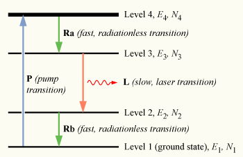
It is easy to realise that it is necessary to have more electrons in the upper level (level 2) than in the lower level (level 1) or else the stimulation will not occur in the required direction. If the number of electrons in level 2 is N2 and in level 1 is N1, N2 needs to be greater than N1. This is called population inversion. However, the number of electrons in each level would normally be governed by the Boltzmann expression and the higher level would be expected to contain fewer electrons than the lower level. Some way must, therefore, be found to increase the number in the higher level and, as this is analogous to filling a water reservoir at a higher level, this is referred to as pumping.
As rather a lot of electrons must be excited between the levels, when there are only two levels, it is best to keep up the population of the higher level at the required steady level by filling it from an even higher level. There will be a steady fall of electrons from this third level. Meanwhile, the population of the third level is kept up by the actual pumping, usually the application of a high electric potential difference – a voltage that supply enough energy to take electrons from the lowest (ground) level up to the third level. The principles are the same whether we are talking about levels in semiconductor lasers or in gas lasers but, in the case of semiconductor lasers, high potential difference means only about 3 V.
As electrons fall from the original level 2 to level 1, the lower level 1 will be filling up. This is not satisfactory and it needs to be emptied it steadily. This is done by having a lower energy level, a fourth level, a bit below the original ground level excited from this level. Then the filling of level 2 is arranged to be fast compared with the movement between levels 2 and level 1, and similarly the emptying of level 1, such that the population ratio N2/N1 (>1) is maintained. Then, we now have a four-level laser.
Structure of a semiconductor laser
In the figure showing the basic structure of a semiconductor laser diode. For example, the active region, which may be of the order of 0.2 m thick, can be gallium arsenide. This is sandwiched with gallium aluminium arsenide, one side being doped p-type and the other side being doped n-type to provide the filling and the emptying. However, the precise processes rely on the principles of pn junctions and are beyond the scope of the present discussion. These layers are deposited on a cleaved substrate and metal contacts are added to both outer surfaces. In the case of gas lasers, pumping is liable to be very inefficient, but in the case of semiconductors there can be 70% efficiency.
SUPERCONDUCTIVITY
In 1911, a Dutch physicist, Heike Kammerlingh-Onnes, was investigating what happened to the electrical resistivity in metals as he reduced their temperature down to that of liquid helium, 4.2 K. He found that the resistivity of platinum levelled out to a constant low value. Impurities in the platinum, however small in number, scattered the electrons and added a finite resistance.
The great surprise came when he used high-purity mercury. Below 4.2 K it appeared to have no resistivity at all, yet on an increase in temperature, the resistivity shot up at 4.2 K. Some important change was happening at this temperature.
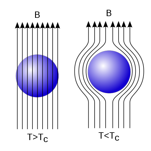
The critical temperature at which mercury becomes a superconductor is called the transition temperature. A metal which can ‘go superconducting’ has a transition temperature below which resistivity drops to zero and it becomes a superconductor. In addition, both the current density in the superconductor and any external magnetic field adjacent to it must be below critical values.
An important application of superconductivity is superconducting magnets which are held at low temperature using liquid helium. The current through the coils of the electromagnets keeps flowing indefinitely and there is no heating of the wire. The magnetic fields produced are exceptionally stable and in medicine are used in scanners for magnetic resonance imaging (MRI) of the human body. Also, the fact that there is little electrical noise in superconductors means that they can be used in low-noise devices.
MAGNETIC LEVITATION AND THE MEISSNER EFFECT
A superconductor can keep a permanent magnet suspended above its surface. As the magnet starts to fall it induces an e.m.f. and hence a current in the superconductor, obeying Faraday’s law: charge flows around at the surface of the superconductor totally unresisted. And, in agreement with Lenz’s law, the effect of this current is to oppose the motion of the magnet, so it remains levitated.
To explain more fully, the current rises to the value that produces a magnetic field which exactly matches and opposes the magnet’s field. The internal ‘supercurrent’ at the superconductor surface can flow continuously and so it behaves as another magnet. Its poles are in the opposite direction to those of the permanent magnet, and the magnets repel. The separation adjusts until the force of repulsion exactly balances the gravitational field.
The field lines of the permanent magnet are excluded from entering the surface of the superconductor, and this is named the Meissner effect. The Maglev train in Japan uses the levitation effect to reduce friction. When a superconductor is placed in parallel lines of magnetic flux, the field lines are pushed out and bend round it. This is not the case for an ordinary metal, nor when the superconductor ‘goes normal’.
Only advanced quantum mechanics can explain superconductivity very well. Actually, I have done some justice to superconductor in one of my very old posts. You can read up more on it here!
Till next time when I discuss more on magnetic materials in relation to condensed matter physics, I remain my humble self, @emperorhassy.
REFERENCES
https://www.britannica.com/technology/transistor
https://en.wikipedia.org/wiki/Transistor
https://en.wikipedia.org/wiki/P%E2%80%93n_junction
https://www.electronics-tutorials.ws/diode/diode_2.html
https://en.wikipedia.org/wiki/P%E2%80%93n_junction
https://www.electronics-tutorials.ws/diode/diode_2.html
https://en.wikipedia.org/wiki/P%E2%80%93n_junction
https://www.physics-and-radio-electronics.com/electronic-devices-and-circuits/semiconductor-diodes/pnjunctionsemiconductordiode.html
https://en.wiktionary.org/wiki/junction_diode#:~:text=Noun,solar%20cells%20are%20junction%20diodes.
https://www.electronics-tutorials.ws/diode/diode_8.html
https://en.wikipedia.org/wiki/Light-emitting_diode
https://en.wikipedia.org/wiki/Semiconductor_laser_theory
https://ehs.oregonstate.edu/laser/training/how-laser-works
https://www.explainthatstuff.com/lasers.html
https://lasers.llnl.gov/education/how_lasers_work#:~:text=A%20laser%20is%20created%20when,orbit%20around%20the%20atom's%20nucleus.&text=Second%2C%20laser%20light%20is%20directional.
https://spie.org/publications/fg08_p94_lasers
https://en.wikipedia.org/wiki/Population_inversion
https://www.britannica.com/technology/population-inversion
https://en.wikipedia.org/wiki/Laser_diode
https://bklein.ece.gatech.edu/laser-photonics/semiconductor-laser-structures/
https://www.fiberlabs.com/glossary/about-semiconductor-laser-diode/#:~:text=The%20basic%20structure%20of%20a,p%2Dn%20junction%20from%20the%20electrodes.
https://www.britannica.com/science/superconductivity
https://www.sciencedirect.com/topics/chemistry/superconductivity
https://en.wikipedia.org/wiki/Superconductivity
https://www.sciencealert.com/superconductivity#:~:text=Superconductivity%20is%20a%20phenomenon%20whereby,efficiency%2C%20losing%20nothing%20to%20heat.
http://hyperphysics.phy-astr.gsu.edu/hbase/Solids/maglev.html
https://www.education.com/science-fair/article/magnetic-levitation-superconductivity-meissner-effect/
https://en.wikipedia.org/wiki/Meissner_effect
Congratulations @emperorhassy! You received a personal badge!
You can view your badges on your board And compare to others on the Ranking
Do not miss the last post from @hivebuzz:
Thanks for your contribution to the STEMsocial community. Feel free to join us on discord to get to know the rest of us!
Please consider supporting our funding proposal, approving our witness (@stem.witness) or delegating to the @stemsocial account (for some ROI).
Please consider using the STEMsocial app app and including @stemsocial as a beneficiary to get a stronger support.