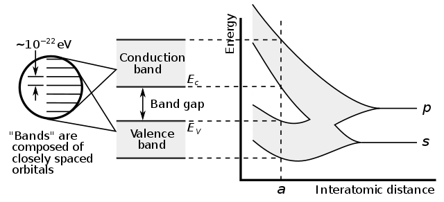
CONDENSED MATTER PHYSICS: Conduction Electrons in an Intrinsic Semiconductor, Thermistors, LDRs and Conduction in a Doped Semiconductor.
Suppose an electron needs energy E to escape from its surroundings, and that this energy is supplied thermally. The temperature T (in kelvin) multiplied by the Boltzmann constant k indicates the amount of energy available to the electron. It can be shown that the number of electrons which acquire enough energy E to jump the energy gap is proportional to e-E/kT.
In fact, for N atoms, each with an electron available to break free, the number of electrons which actually do so is given by:
n = Ne-E/kT
The expression e-E/kT, which gives the ratio of the number of electrons excited to the total number of existing electrons available for excitation, is called the Boltzmann factor and this same factor exists in other examples of thermal activation. Another common example of a process where this factor comes in is diffusion, where an atom or ion needs to be excited above an energy barrier before it can jump to an adjacent site.
The number n rises rapidly as the temperature T increases. It is these electrons which reach the conduction band and allow electrical conduction in a semiconductor. The resistance of a semiconductor decreases as the number of carriers increases: double the number of carriers, and the resistance halves, and so on. It is not difficult to see that the resistance will vary proportionally to eE/kT
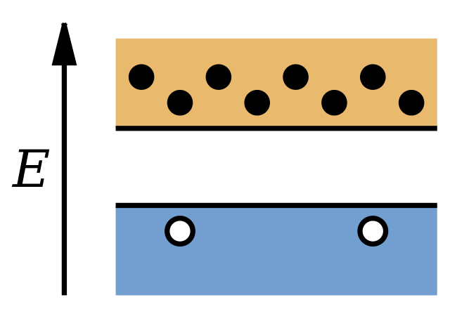
Additionally, by escaping from the lower valence band, each electron leaves behind a gap called a ‘hole’. We can liken this effect to a passenger moving from a bus queue on to the bus. In the queue, as a person leaves, the rest move up, one by one, to fill the gap left by the previous person. You will see a gap move down the queue in the opposite direction to the actual movement of the passengers. Similarly, in the valence band of the semiconductor, once a gap or hole is left, an adjacent electron can jump into it. Applying an e.m.f. to the semiconductor makes electrons jump like this. With repeated jumps of electrons, one after another, holes move through the semiconductor in the opposite direction to the electrons.

Electrons move under the influence of the e.m.f. towards the positive potential (Corresponding to the bus-stop sign), while the holes in the valence band move the opposite way. It is as if the holes have a positive charge. So we say that such a semiconductor has electrons in the conduction band and holes in the valence band and that both act as carriers of charge. The electrons move against the electric field as they have negative charge, the holes move with the field as they are of positive charge.
We get the overall conductivity by adding together the contributions from both types of charge. Their contributions must be added as, although they have opposite charge, they also move in opposite directions. When electrons that are excited into the conduction band leave behind an equal number of holes, we describe the semiconductor as intrinsic and the conduction as intrinsic conduction.
Because far fewer charges move in a semiconductor than in a metal, a semiconductor has a lower electrical conductivity. This lower conductivity is slightly offset by the ‘mobility’ of the electrons (their ability to move in an applied e.m.f.), which is much higher for a semiconductor than for a metal: the drift velocity of semiconductor electrons is usually many metres per second.
As the temperature of a semiconductor is increased, the mobility of the electrons (and the holes) decreases, just as it does in a metal. But the increased temperature enables more electrons to be excited from the valence to the conduction band. This effect happens rapidly as the temperature effect is exponential and it swamps any variation of the mobility. Overall, as temperature rises, the increased number of carriers increases the conductivity of the semiconductor.
EXAMPLES OF SEMICONDUCTOR MATERIALS
Typical semiconductor materials are the elements silicon and germanium, with atoms in a structure like that of a diamond. The atoms are covalently bonded, meaning that adjacent atoms share outer electrons and come from Group 4 of the Periodic Table.
For silicon, the bandgap is 1.1 eV and for germanium it is 0.67 eV. kT measured in eV at room temperature is 0.026 eV, that is, (8.6 × 10-5 × 300) eV.
Another commonly used semiconductor material is the compound gallium arsenide, with a bandgap of 1.43 eV. Gallium is from Group 3 and arsenic from Group 5. The atoms take up alternate sites in the diamond structure and are also covalently bonded: adjacent atoms share electrons (unlike ions which lose or gain electrons).
Compound semiconductors are similar in behaviour to single-element conductors. For example, although gallium arsenide is a more complicated material to prepare and to use than single-element semiconductors, it is popular. The reason is that the electrons move through gallium arsenide very much faster than they do in silicon or germanium, so devices operate more rapidly. Other, less used, semiconductor materials contain atoms of three different elements.
By altering the proportions of elements and compounds, semiconductors can be made with the right bandgaps for their use. For example, semiconductors used in infrared cameras can be made to detect light of infrared frequency. The incoming photons of light each have an energy equal to the semiconductor bandgap energy and are absorbed as they excite electrons up across the gap. In reverse, light is emitted by semiconductor lasers that are designed to produce light of a particular frequency and colour. They are used in CD players and for optical communications.
THERMISTORS AND LIGHT-DEPENDENT RESISTORS
Thermistors detect variations in temperature and so are rather Iike thermometers, while LDRs, light-dependent resistors, detect variations in light level. Varying the temperature of thermistors changes the number of available electrons for conduction, while incoming light alters the number in LDRs.
A thermistor is made of a semiconductor material such as nickel oxide. Its resistance very rapidly decreases exponentially (not linearly) as its temperature rises because the number of free carriers increases exponentially. As we have seen, increasing the temperature, and hence thermal energy excites more electrons into the conduction band. Because of this rapid change of their resistance, thermistors are useful for measuring temperature.
A typical variation of resistance for a thermistor is from 4.7 kΩ at room temperature to 270Ω at 100 °C. So thermistors are used in electronic circuits where big changes of output signal are required for small variations in temperature. For example, a thermistor can be used with a computer to monitor a process that produces thermal energy, such as a chemical reaction. Belng Sensitive to a tiny energy change, the thermistor gives rise to a large input signal that is used to record and control the process.
LDRs are usually made of cadmium sulphide which has a bandgap of 2.6 eV – larger than the bandgap for a typical semiconductor. For LDRs, it is photons of light which provide the energy to excite the electrons irom the valence into the conduction band. The dark resistance of an LDR is typically 1 MΩ, and this decreases with increasing light intensity to 1 kΩ or less, depending on the magnitude of intensity. LDRs are also easily incorporated into electronic circuits.
CONDUCTION IN A DOPED SEMICONDUCTOR
The precise conducting properties of semiconductors used for transistors, thermistors and LDRs are controlled by adding very small amounts of ‘impurity’ which is a very tiny quantity of another element. The process of adding the impurity is called doping and the extra material is the dopant. Dopant atoms go into positions in the original semiconductor lattice to replace a few of the atoms of the pure material. Their size must be similar to the size of the atoms they are displacing. Assuming I start with a group 4 semiconductor such as silicon, then I choose either a Group 3 element such as boron or a Group 5 element such as arsenic or phosphorus. Choosing to replace with a Group 3 or a Group 5 element leads to quite different changes.
Arsenic-doped silicon
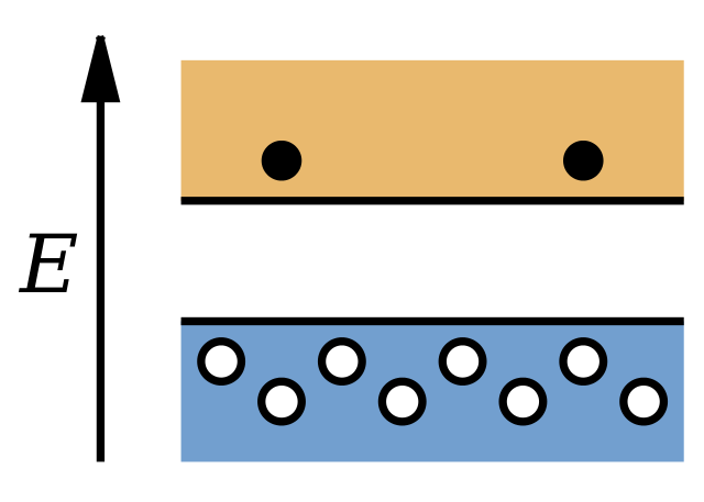
Starting with a lattice of silicon atoms, each atom shares its outer four electrons with four other atoms and shares a further four electrons from its neighbours to establish a filled shell of eight electrons. Conductivity occurs when some of the electrons are excited thermally into the conduction band. If I now replace a few silicon atoms with arsenic, each arsenic atom brings with it an extra electron. This extra electron in arsenic is easily excited into the conduction band. For the bulk material, the band structure diagram shows these extra arsenic electrons within the energy band diagram just below the conduction band.
At room temperature, they are thermally excited up into the conduction band. By controlling the number of dopant atoms we can control the number of current-carrying electrons and hence the conductivity. The dopant atoms are referred to as donors because they are giving up electrons and the semiconductor is called n-type because it has negative-type carriers.
Boron-doped silicon
I can instead add boron atoms as a dopant. They have one electron less than the silicon atoms and the lattice can easily take up electrons from the valence band. This leaves holes in the valence band to carry current. The boron atoms are called acceptors as they are taking up electrons and the semiconductor is called p-type (positive carriers). The acceptors on the energy band diagram can be represented at a level just above the valence band.
A semiconductor in which the conduction is dominated either by electrons from donor atoms or by holes from acceptor atoms is called an extrinsic semiconductor. We can either have an n-type semiconductor in which the carriers are predominantly electrons or a p-type semiconductor in which the carriers are holes. For either case, we can find out the number of carriers by measuring the Hall voltage.
More on this and some others will be discussed in my next post. Till then, I remain my humble self, @emperorhassy.
REFERENCES
- https://en.wikipedia.org/wiki/Intrinsic_semiconductor
- https://www.physics-and-radio-electronics.com/electronic-devices-and-circuits/semiconductor/intrinsic-semiconductor/conduction-in-intrinsic-semiconductor.html#:~:text=In%20intrinsic%20semiconductor%20the%20number,of%20hole%20and%20electron%20current.
- https://en.wikipedia.org/wiki/Semiconductor#:~:text=Some%20examples%20of%20semiconductors%20are,frequency%20integrated%20circuits%20and%20others.
- https://www.bbc.co.uk/bitesize/guides/zcgkp39/revision/5
- http://www.schoolphysics.co.uk/age14-16/glance/Electricity%20and%20magnetism/LDR_and_thermistor/index.html#:~:text=This%20is%20a%20type%20of,means%20a%20drop%20in%20resistance.
- https://opentextbc.ca/universityphysicsv3openstax/chapter/semiconductors-and-doping/
- https://courses.lumenlearning.com/introchem/chapter/doping-connectivity-of-semiconductors/#:~:text=Semiconductor%20Doping&text=p%2Dtype%20dopants%20assist%20in,easy%20formation%20of%20positive%20holes.
- https://aip.scitation.org/doi/pdf/10.1063/1.5025516
- https://electronics.howstuffworks.com/diode1.htm#:~:text=N%2Dtype%20%2D%20In%20N%2D,get%20into%20the%20silicon%20lattice.&text=Boron%20and%20gallium%20each%20have%20only%20three%20outer%20electrons.
- https://en.wikipedia.org/wiki/Doping_(semiconductor)
- https://www.hindawi.com/journals/jnm/2012/912903/
- https://www.halbleiter.org/en/fundamentals/doping/#:~:text=Doping%20means%20the%20introduction%20of,electrons%20%3D%205%2Dvalent).
Thanks for your contribution to the STEMsocial community. Feel free to join us on discord to get to know the rest of us!
Please consider supporting our funding proposal, approving our witness (@stem.witness) or delegating to the @stemsocial account (for some ROI).
Please consider using the STEMsocial app app and including @stemsocial as a beneficiary to get a stronger support.