Ben Eater 6502 Kit — Day 16
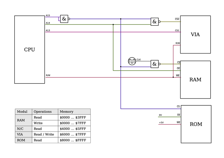
Ben Eater used a single SN74H00N 4×2 NAND chip as memory management unit which decoded 3 address lines (A13 … A15).
This saves integrated circuits but has a few drawbacks and quirks:
- The VIA uses up 8kb of memory
- 8kb of memory is unused
- Only half the 32kb of RAM are usable
- Write operations to the VIA are also written to the RAM
Im not doing anything about the latter. It's not that unusual as the C64 did something similar. Speaking of the old 8bit day: All systems I know of used only 256 byte of address space for any I/O chip. So that's the goal I have set myself:
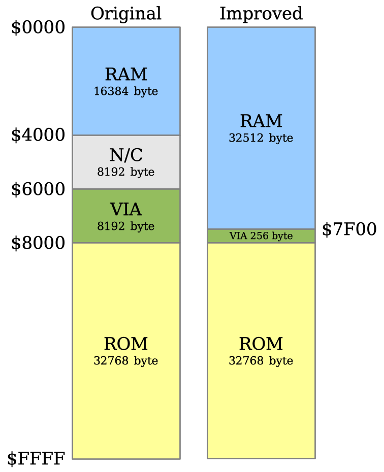
Improvement planned
In order to get the VIA usage below 256 bytes 8 address (A8 … A15) lines need to be decoded. This can be done with an SN74LS21N 2×4 AND. The circuit I came up with looks like this:

Improved memory management unit
It's pretty simple a straightforward and I was even able to save one of the NAND gates. Only problem is that the SN74LS21N is not one of the common circuits. Next step is to actually wire up:
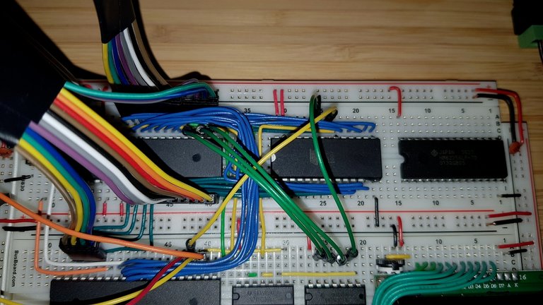
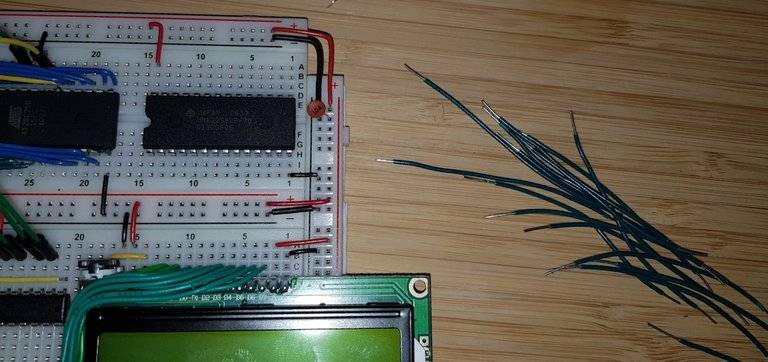
Plug the RAM in
Intermediate MMU with temporary wiring
Lots of wires
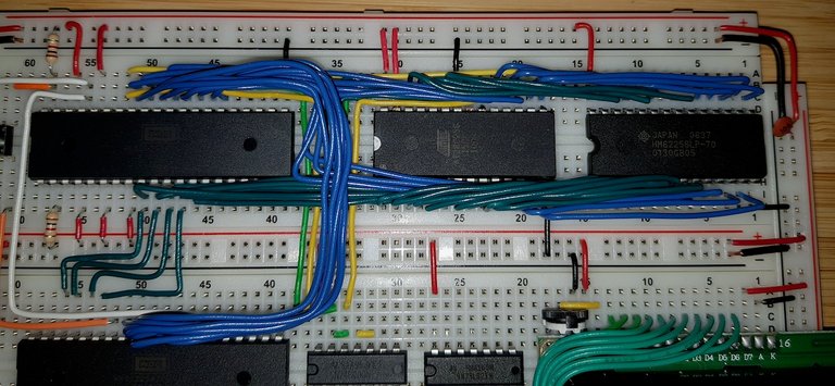
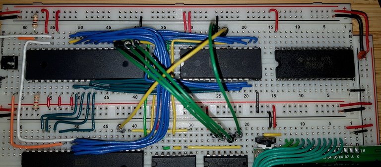
Address bus and data bus wired up
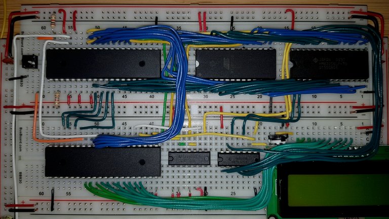
Everything done.
PS: Yes, I'm using the new IEC 60617-12 : 1997 symbols for logic gates. I'm a German and I always found the US symbols overly complicated and easy to mistake if hand drawn. The German symbols where a little better in that regards. But they are still difficult to draw with a drawing software. While the new IEC symbols have a simple elegance to them.