Back to the Bad Old Days of Programming - Book Project Post I
Overview
One of my current projects is a book covering DIY computer system design for readers who have little knowledge of electronics. There are plenty of books and online how-tos out there instructing people to find the nearest hobbyist/"maker" board (Raspberry Pi, Arduino, etc), download some prewritten code into an IDE, compile it, and load the code into the board's flash. This is fine to learn the very basics of software compilation, IDE use, etc but is neither engineering nor design. My project focuses on the design of a computer system and engineering, taking the reader from nothing but a pile of components, a schematic capture/PCB layout program, and soldering iron through to a functioning computer. Granted, due to technical and other limitations and considerations, the computers presented are all 8-bit based on either the 8085 or Z80 (reader's choice). Very retro at a time retro seems to be popular again. This series of posts will be behind the scenes work I think some will find interesting, rather than content from the book itself.
While most of the work done so far for the book has been hardware related, some development and testing has been completed on the firmware side. It would be easy to port the RTOS I wrote for use in personal and client projects over to this system; however, it is closed-source (Amazon, the Chinese, etc steal everything thats not bolted down) and goes against the idea of building something (including firmware) from nothing. The firmware is split into serveral stages, mainly to minimize the amount of machine code the user needs to manually enter by directly manipulating the system busses.
Hardware
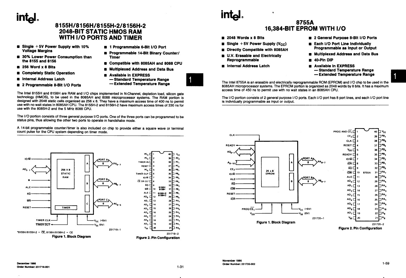
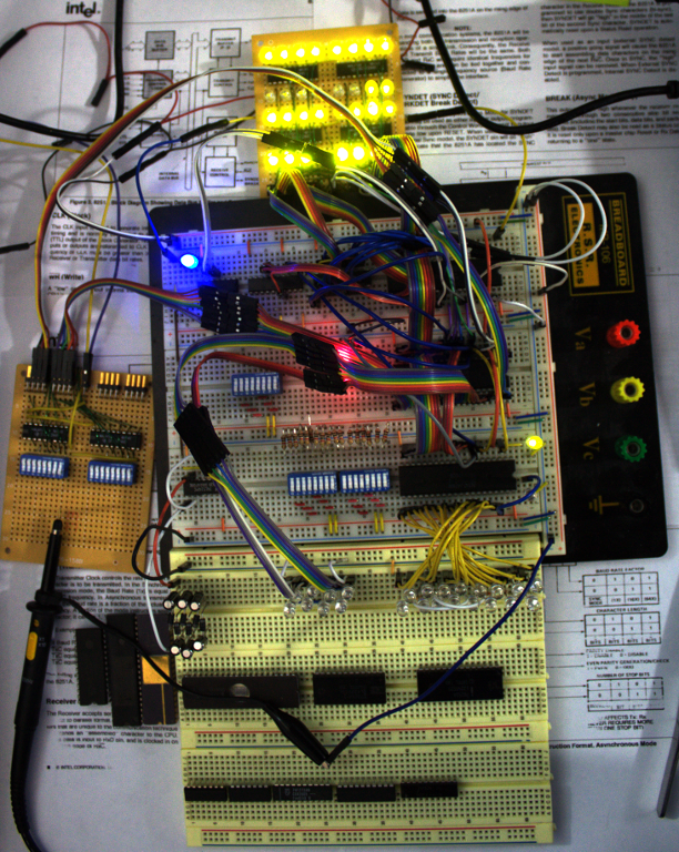
The simplest system is based on the 8085 and several MCS-85 support chips, specifically the 8155 and 8755. The 8155 is a 256 byte RAM with two 8-bit I/O and one 6-bit I/O port and 14-bit timer. The 8755 is a 2kB EPROM with two 8-bit I/O ports. After considering various requirements, the decision was made to include three 8155s and a single 8755 in the system. This gives a total of 768 bytes of RAM and 2kB or EPROM.
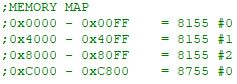
Figure 1 - Memory map
The memory map and I/O map are shown in Figures 1 and 2 respectively; however, it is important to note the 8755 will be swapped with 8155 #0 after firmware has been witten to it. The reason for this is that the 8085 begins execution at address 0x0000, and we will initially only be able to load firmware into RAM via manual entry.
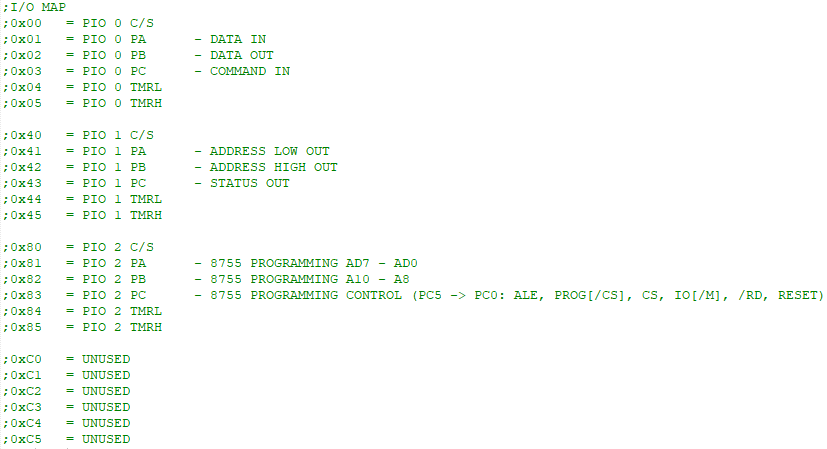
Figure 2 - I/O map
Clock generation is simple RC-based circuit, consisting of two 7414 schmitt trigger inverters, a resistor, and capacitor. This was done to keep things inexpensive and to allow the user to easily change the clock frequency by changing the value of the resistor, capacitor, or both. Figure 3 illustrates the clock generator.
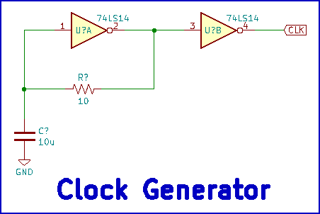
Figure 3 - Clock generator
Figure 4 shows the CPU block, consisting of the 8085, a LED to indicate when the CPU is in the hold state, and a switch to reset the system as well as a switch to place the CPU in the hold state. All interrupt lines are tied inactive (logic 0) because interrupts are not used at this stage of the system's design.
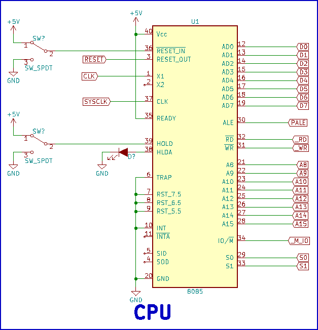
Figure 4 - CPU
Because the CPU does not place ALE into high-impedance during hold states, it is necessary to use external logic to allow the user to control the level of ALE during manual programming and bus control. A 7432 OR gate is used for this purpose, combining the processor ALE (PALE) and manual ALE (MALE) signals to produce the final ALE signal. This circuit, along with a circuit to indicate when the CPU is in the halt state, is shown in Figure 5.
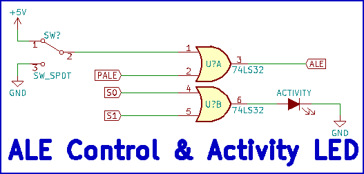
Figure 5 - ALE control & activity LED
With the 8085, the low-order address byte is multiplexed with the data bus, so a register must be used in conjunction with ALE to latch the low-order address when it appears on the data bus. This is shown in Figure 6.
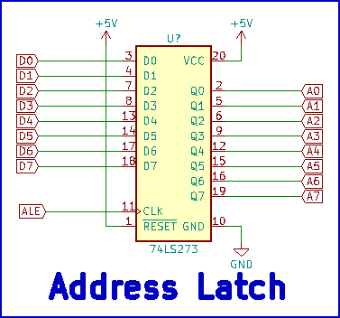
Figure 6- Address latch
The chip select mechanism, shown in Figure 7, is implemented using a 74138 3-to-8 decoder and is wired to provide the chip select signalling already covered in Figure 1. The reason a 74138 is used rather than a 74139 decoder is for future expansion of I/O ports that will provide additional functionality to the system.
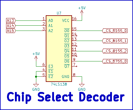
Figure 7 - Chip select decoder
In the initial implementation of the system, only two 8155s are used. One is to accept commands as well as accept data from and present data to the use, while the other is used to display the current address and command lockout indicator. Figure 8 illustrates which ports are used for input and display functions. 8155 #0 Port A is used for data input, Port C of the same chip is used for command inputs, and the chip's Port B displays data. Ports A and B of 8155 #1 display the address and a single bit of Port C displays the lockout indication.
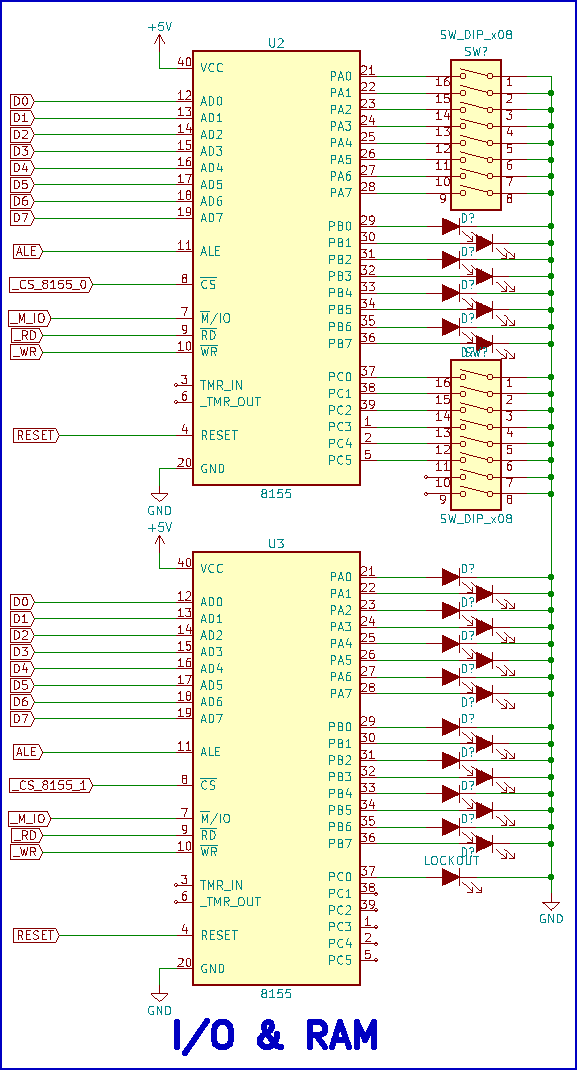
Figure 8 - I/O & RAM
The last circuits to cover, in Figure 9, before moving on to the firmware are the DIP switches used to manually control the system busses as well as the LEDs used to display the state of various bus signals. Because the 8085 uses a multiplexed bus, a only single DIP switch is needed to enter data and the low-order address. The remaining DIP switch is used to enter the three highest-order address bits (A15 - A13), select between I/O and memory, and select read or write operations.
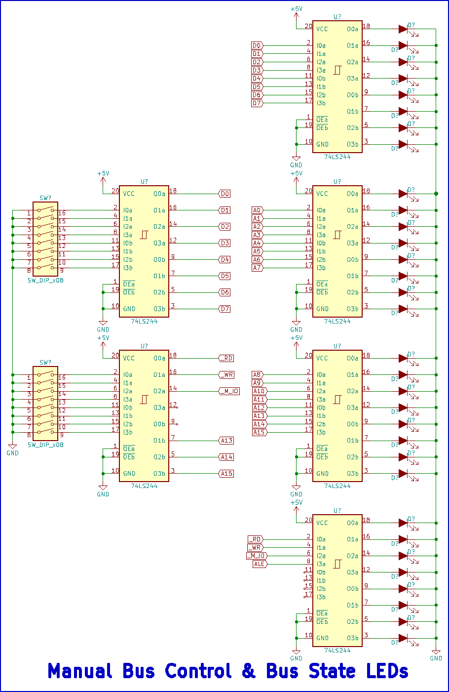
Figure 9 - Manual bus control & LEDs
To reduce the number of LEDs and DIP switches required for this implemenation, the user may choose to move the switches and LEDs from the manual bus control arrangement (Figure 9) to the command-based arrangement (Figure 8) once the command system firmware has been entered into memory.
Firmware
The first-stage firmware has only one purpose, to eliminate the need for the user to manually control system busses while entering machine code. I first considered the command structure as I sat in a vehicle atop the parking structure at Keck Medical Center while waiting for my father to have some outpatient work done to treat his cancer. I usually keep a small binder contaning a pen, graph paper, and a few key datasheet pages for whatever components are in the project I am working on.
Commands are entered into the system via a DIP switch connected to a 6-bit I/O port; therefore, only six bits are available to implement commands. Two easy options exist for command formatting, one is to assign each command a unique bit and the other is to encode each command using a unique combination of the six bits. The former method is easier for the user to remember as well as implement in code, so that method was explored before looking at the latter method. One could first determine the number of commands needed, then select how those commands will be entered, but I often find it better to develop things under the more restrictive regime then add features as needed. What are the basic commands required to get the first-stage firmware operational, and can we limit them to six or less?
The user needs to be able to do the following things:
- Load an address to display the contents of, write data to, or execute code from
- Load data value to write to an address
- execute code at an address
Three commands are the minimum to get the system working as intended; however, because the decision was made to use a single DIP switch to enter data value, the address load command must be split into two commands:
- Load low-order (LSB) address
- Load high-order (MSB) address
This brings the total number of commands to four, leaving room for two more. What sort of commands would be helpful for the user? What would abstract more hardware from the user's view? The answer lies in the fact that with the current commands the user will need to manually increment addresses when they need to enter machine code at the next address. More specifically the user will need to manually load a new low-order address byte for each byte of machine code entered into memory, or in the worst case load both address bytes. Therefore, commands to increment and decrement the address will be helpful, giving the following commands:
- Load the active address (low-order byte)
- Load the active address (high-order byte)
- Increment the active address
- Decrement the active address
- Write data to the active address
- Execute code located at the active address
If you have been paying close attention, you will notice some of the terminology changed between the initial command list and the final command list. This is because a method is also needed to view the contents of memory locations. While this could be its own command, it is simple to have the firmware automatically display the contents of memory locations when a new address is loaded. Thus the result is a system in which all operations work on data in (or transfer control to) locations specified by an active address chosen by the user.
To set the active address, the user performs the following:
- Sets the data DIP switch to the value needed for the LSB of the address
- Activates the load active address (LSB) command switch
- Sets the data DIP switch to the value needed for the MSB of the address
- Activates the load active address (MSB) command switch
It is not important what order the address bytes are loaded in, steps 1 & 2 may follow steps 3 & 4 if the user desires.
To increment or decrement the active address, the user simply activates the respective command switch. Loading data is similar to loading an address, but takes only two operations:
- Set the data DIP switch to the value required
- Activate the write data to active address command switch
Forcing the system to transfer control to code located at the active address is as simple as activating the execute switch.
One last mechanic must be considered, how will the system know when the input it receives from the command switches is valid? Given the low system clock frequency, debouncing is not an issue. However, will the system immediately carry out a command when a command switch goes active, or will it wait until the command switch goes inactive again? The former option can create a condition where the command finishes executing while the command switch is still active, then immediately executes the command again. Therefore, the latter option will be used where the user must return a command switch to inactive before a command is processed. In fact, before a command can be accepted, all command switches must be inactive. Finally, if more than one command switch is active when a command is accepted, the one with the highest priority will be procesed and the other ignored.
The Programming
A number of subroutines compose the firmware which allows other code to use the common subroutines. Turning the command LED lock on and off are very simple routines and shown in figure 10.
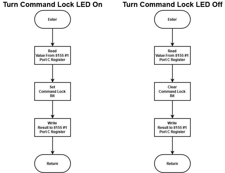
Figure 10 - Command lock LED on & off subroutines
Figure 11 shows the two subroutines used to ensure commands are valid, as previously discussed. One subroutine waits for all command switches to go inactive, and the other waits for any command switch to go active.
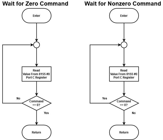
Figure 11 - Wait for zero and non-zero command subroutines
After a command is accepted it must be decoded, which is a straightforward process of computing the first set bit in the command byte. For example, if bit 0 is set the command index will be zero, and if bit 4 is set the index will be four. Because a method is needed to distinguish a valid value for the command byte from an invalid one, the CPU's carry flag (CF) is set when an invalid command is entered. Figure 12 shows the program to accomplish this, which consists of a loop that shifts the command byte right into the CF until a set bit is encountered, then computes the bit's index by subtracting the number of shifts from the total number of commands.
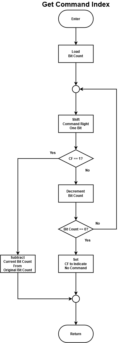
Figure 12 - Get command index subroutine
The main program is shown in Figure 13, which starts by loading the stack pointer (SP), setting the active address to 0x0000, and cofiguring both 8155 PIOs. After this the main program loop is entered, where the command lock LED is turned on and the active address is displayed to the user. The caveat here is that this is the formal main loop. Another loop exists as an informal line of control flow back to the top of the main loop from whatever command has been completed. This will be covered later. Data is read from the active address and displayed to the user then the program waits for the command switches to all be in the inactive state. After this happens, the command lock LED is turned off and the program waits for one or more command switches to go active.

Figure 13 - Main program
At this point the program enters an inner loop that waits for the command switches to go inactive. The command byte is saved along with whatever value is present on the data DIP switch, and that value is displayed to the user. Another read of the command DIP switch is performed, with the program jumping back to the top of the inner loop if the value of the command byte is not zero. When the command switches all go inactive, the software begins processing the command byte by setting turning the command lock LED on and computing the command's index. The bottom of the formal main loop is formed by a check for a valid command. If the command byte contained no valid commands, program flow continues at the top of the main loop.
In preparation to execute a valid command, a return address is pushed onto the stack. This return address points to the top of the main loop, forming the previously mentioned informal loop. Rather than invoking a command by directly calling its subroutine, a table structure holding the address of each command is used. To find a command's execution address in this table, the command's index is multiplied by two then added to the table's base address. Loading the command's execution address and pushing it onto the stack are the next steps, followed by an informal call to the command by executing a return instruction.
Because of the simplicity of each command, their programs are not listed here, but their code can be found in the next section.
The Code
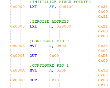
Figure 14 - Initialization code
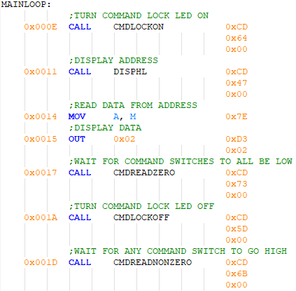
Figure 15 - Top of the main loop
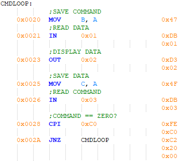
Figure 16 - Inner loop
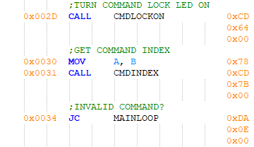
Figure 17 - Bottom of main loop
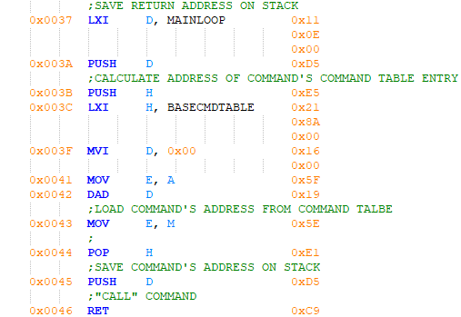
Figure 18 - Invoking a command
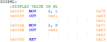
Figure 19 - Display the value in HL
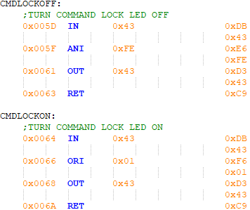
Figure 20 - Command lock LED on/off
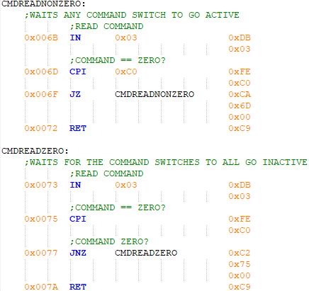
Figure 21 - Wait for command switches to go active/inactive
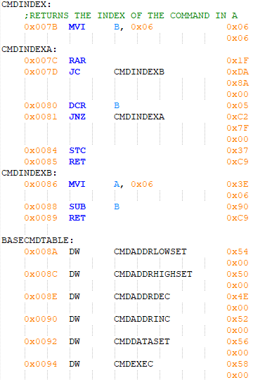
Figure 22 - Calculate command index and command table
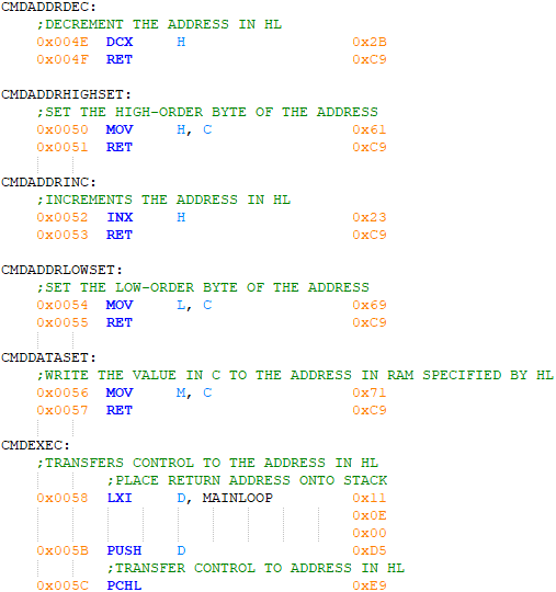
Figure 23 - Code implementing the six commands
In closing, below is a video of the first stage firmware in action
If you have questions, feel free to ask me in the comments below. I will do my best to answer good questions, if the website does not give me grief like it did a while back when someone asked a question. However, if you ask me how does the 8085 work, what certain opcodes do, etc -- there are datasheets and books for that. Please consult them. In addition, I have a video covering the 8085 and its instruction set:
Posted with STEMGeeks
Congratulations @tacticalcadaver! You have completed the following achievement on the Hive blockchain and have been rewarded with new badge(s) :
Your next target is to reach 2250 upvotes.
You can view your badges on your board and compare yourself to others in the Ranking
If you no longer want to receive notifications, reply to this comment with the word
STOP