Logic circuit using "Logisim" (RS-232 Protocol)
I am a student of electronic engineering from the Simón Bolívar University of Venezuela, a few months ago I was in the course of "Digital Circuits" where we were evaluating the design of logic circuits through different simulators including the simulator "Logisim" . One of our evaluations was to implement the RS-232 protocol to send the selected number on a matrix keyboard.
Objective:
Implement a protocol similar to RS-232 to send the previously selected number on a matrix keyboard.
Design:
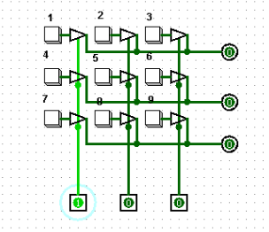
We received the design of a 3x3 size matrix keyboard excited by pins connected to each column of the keyboard respectively, once the column is excited, one of the three available buttons in that column can be selected, when more than one column is on at the same time, if a number is selected on the keyboard the circuit’s output will be invalid, then the circuit originally delivered:
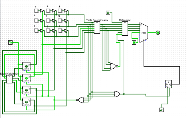
The three columns were connected to the output of three flip flops type D, these works as a future state of the same, a flip flop D was added (referred to as column zero (C0)) C1, C2 and C3 being the columns listed from 1 to 3 from left to right to start the state machine when each flip flop marks zero. In this way the three columns will be lit one by one.
These 4 outputs of the flip flops that works as a future state, enter the integrated circuit: "Excita columnas" which throws the following state of the columns in the output.
The circuit obeys the following truth table:
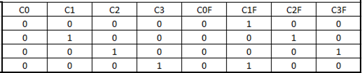
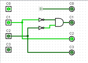
Resulting in the following circuit:
In this way the columns are enabled one by one without ever matching.
Design of the logic circuit that determines which of the keys has been activated:
The rows activated by pressing any button on the keyboard are the following:
F1: Corresponding to the row activated by buttons 1,2 and 3.
F2: Corresponding to the row activated by buttons 4,5 and 6.
F3: Corresponding to the row activated by buttons 7,8 and 9.
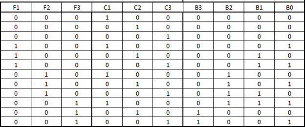
The columns that excite the keyboard (C1, C2 and C3) and the rows activated by it (F1, F2 and F3) when a key is pressed will be connected to an integrated circuit "Tecla seleccionada" that receives these parameters as input, to the output is given a number in binary coding, represented by the terms: B3, B2, B1 and B0, with B3 being the most significant bit, this in order to create column-row combinations that represent the number of the selected key.
The circuit is governed by the following truth table:
Resulting in the following circuit:
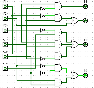
In this way, when you press a button, it will coincide with the columns excited by the keyboard that will vary and say the selected number in binary coding.
Similarly, the cables at the keyboard output were connected to an NOR gate, which connects its output to the “Enable” of each type D flip flop, this to stop their work and maintain the current state that is being presented .
Following is the state diagram of the state machine:

Where the numbers represent the current state of each column of the matrix and the extra flip flop that I have called Co. Which govern the behavior of the circuit input.
Logic circuit design that, for each key pressed, sends the key number via serial using the RS-232 protocol:
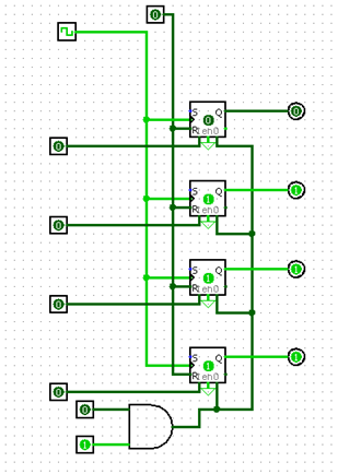
At the output of the circuit “Tecla seleccionada” there is another integrated circuit called “Retenedor”, it is composed of an arrangement of SR type flip flops, which are responsible for retaining the value that the circuit “Tecla Seleccionada” throws even when This flies to its idle state, in this way the binary encoding of the selected number on the keyboard is obtained at the output of the retaining circuit, remaining as follows.
Once the selected number is retained, it is connected to a multiplexer occupying its inputs from zero (0) to three (3) and attaching a fourth bit which will be set to 1 as the stop bit.
We were specified that the transmission rate should be 100 baud, therefore the ratio was used to calculate the “tick” of the clock of T = f / 2 (N-Baud) obtaining a “clock” of 10 “ticks” as rising and falling edge, this was connected to a counter, previously set to its maximum value which is 4, which will count from 0 to 4 when it is returned to zero, to encompass the 4 transmitted bits and a stop bit at the moment a number is selected.
Likewise, an NOR gate was connected to the 4 outputs of the “Selected key” circuit, which also connects its output to the “Retainer” circuit, this to be able to connect with the flips and be able to perform logical operations to be able to retain the selected number, this can change if another key is selected.
As it was done at the entrance of the circuit “Tecla Seleccionada”, the three outgoing rows of the matrix keypad were taken to connect to a logic gate in this case OR, whose output was directed to the “Clear” of the counter, in this way the counter it will return to zero each time a key is selected and thus be able to start the count which is related to the multiplexer so that each of the bits can be read from the most significant to the least significant.
Finally obtaining the following circuit:
Results:
At the output of the multiplexer, the result of serially transmitting the selected number is observed when any key is touched, the counter will be reduced to zero and will begin to increase at a transmission rate of 100 baud, so that the multiplexer can display at output each of the bits corresponding to its position at the input thereof, in this way shows each number selected in binary coding starting with the most significant bit and will conclude with the stop bit which was previously set to 1.
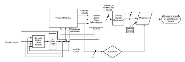
Below is the diagram of the circuit blocks:
Conclusions:
It was possible to implement a circuit that fulfilled the specified task since it was possible to perform the bitwise transmission in a similar way to the RS-232 protocol, the circuit that excites the matrix keypad was prepared in an appropriate manner and the number selected for It can be transmitted bit by bit with the help of a multiplexer. However, it should be noted that by keeping a key pressed the bit-by-bit transmission will begin when it is released, which makes the result later if it is in these conditions, otherwise the circuit works correctly according to the requested specifications.
References:
Ángel Terrones, “Circuit Q2” delivered on 12/22/18.
Spartan-3 FPGA Starter Kit Board User Guide, UG130 (v1.2) June 20, 2008.
Taub, Herbert. Digital Circuits and Microprocessors. Calypso editorial. Mexico DF. (1998)