Transmission Electron Microscope: Principle and Working |ChemFam #13|
Greetings to everyone! It’s a pleasure meeting you all again. In my previous post, I wrote about functioning and working of SEM. Today, I will be discussing about another class of electron microscopy i.e., Transmission electron microscopy (TEM).
As the term itself suggests that we will be utilising transmission mode of electrons to find out the features or to look inside the material. In this particular case, we want the material to be transparent to electrons; so that the electrons gets transmitted through the material and provide some information about the material itself.
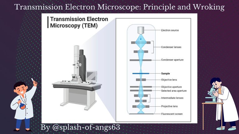
The transmission electron microscopy (TEM) is a microscopy technique which uses a focused beam of electrons transmitting through a specimen to form an image. The image then reads all kinds of characteristics of the sample that are required for research purpose. The specimen is most often an ultra-thin section having a thickness less than 100 nm or could be a suspension on a grid. The electrons interact with the sample and due to the interaction, an image is formed as the beam passes or transmits through the specimen. The image is then magnified and focused onto an imaging device which can be a fluorescent screen or a sensor such as a scintillator attached to a charge-couple device.
Principle:
The working principle of TEM is not very much different from light microscope rather similar. Although, major difference is that light microscope uses light rays as a source to focus and produce an image, whereas TEM uses a beam of electrons to focus on the specimen to produce an image.
Electron Interaction:
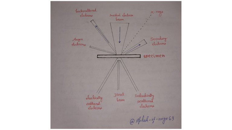
The electron interaction around the specimen in a way that if we have a specimen then we get some electrons which are inelastically scattered. These electrons can either be secondary electrons or auger electrons or sometimes they can also elastically scattered back after interaction with the specimen and we get them as backscattered electrons. Thus, once we apply electron beam, we can get some signals which are coming back either as secondary electrons, auger electrons or backscattered electrons. They can also interact with the sample to produce something called X-rays. Now, these are all happening above the sample regime. They are not allowing the electrons to pass through the material.
What if the material we have is transparent?
If we have a material that is transparent enough or thin enough through which we can attain transparency for the electrons to pass through the material. In that sense, we can get the incident electron beam. We can let it pass through having high energy so that it comes out as a direct beam or it can also get inelastically scattered. We can also detect the inelastically scattered electrons, but we do not really need them. Why? because once we are supplying certain kind of energy to the material and the electron is undergoing some inelastic losses, so we do not know what is the input. Though, we know what the output is we will not know what the input energy of electrons. So, we will not know their wavelengths. Thus, we will not be knowing overall functionality of how they are interacting with the material, but we are finally getting some signal.
In some cases, we can tap those particular signals which might help in the overall analysis of the structure of the material or to track some of the crystallographic directions. But again, we will be getting much more informations if the electrons are getting elastically scattered in the sense that we now know both the input and output.
Diffraction pattern:
For a micron sized particle, generally we always get some diffraction peak. So for a microcrystalline with a grain size greater than 1 micron, We will be seeing some peaks which are associated with a particular diffraction angle value and hence we will be getting some certain intensity from the crystal which in turn provides some information about the sample. But as soon as the material starts becoming much more nano crystalline or some micron size then what happens?
In that case the XRD(X ray diffraction) crystallography is not able to detect whether we have some crystallinity into the material. It rather starts showing broadening of the peak. Because as soon as my grains are becoming finer and finer, I start getting broadening of the peaks. But, I do not know whether the broadening is either because I have an amorphous material or the crystals have become nano crystalline in nature. So, that complexity can be easily analysed by TEM. Thus, in TEM, we can image and analyse all these nano crystals.
Advantage of TEM over XRD:
From the electron diffraction we can probe a very small area that can be a nano crystal and we can obtain an electron diffraction pattern. Because now our beam is much more refined and we are letting the electrons to interact with the material instead of an x ray. The x ray will interact with the cloud of an electron or an atom as a whole. But electrons are so sensitive that once we are sending an electron to interact with the material it gets diffracted even by a single electron or the positive charge of the nucleus. So we can get a very strong signal if we let electrons interact with the material and point it towards single nano crystal and that is what gives us the diffraction pattern. So, in XRD many many grains contribute to the overall diffraction field, but in our electron diffraction field we can let small beam of electrons to interact with the particular nano grain and we can get a diffraction pattern out of it.
Beauty of TEM: Ewald Sphere
As we have discussed already that the electron interaction with the material is much more stronger. So, it is approximately 106 to 107 times stronger than those of x rays. Eventually our diffracted electrons will have a very high intensity. The Ewald sphere which basically provides the diffraction pattern having radius given by 1/λ. The wavelength in TEM is approximately 2 picometers whereas, in x rays is approximately 100 picometers. So, we get a bigger radius for the Ewald sphere which makes the sphere much flatter. Hence, more number of points starts interacting with the Ewald sphere and produce a diffraction spot. Now yet again as the wavelength decreases the diffraction angle also gets reduced. This can be verified by the Bragg’s equation which is 2d sinθ = n λ. So the diffracted range will be very very near or they will be within a range of few 0 to 1 degrees. So that tells us that we can get all our diffraction patterns within tilt of a particular plane which is only 0 to 1 degree along the beam.
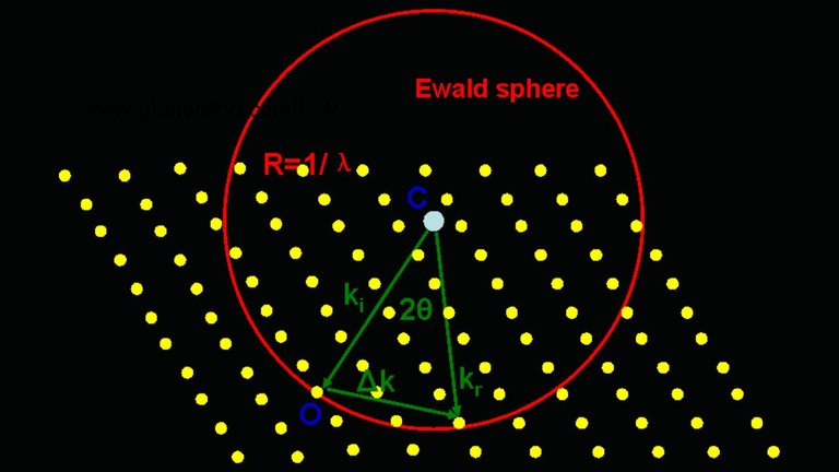
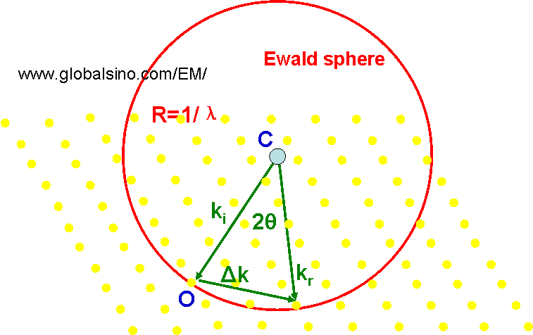
One more thing about it is since the intensities are very strong because electrons will interact very strongly with a particular matter. So, the exposure time automatically gets reduces to only a few seconds.
| TEM | X-rays | |
|---|---|---|
| Wavelength | ~2 pm | ~100 pm |
| Diffraction angle | ~0-1 degree | 0-180 degrees |
| Interaction with electron cloud | Scattered by positive potential inside electron cloud | Interact with the electron cloud |
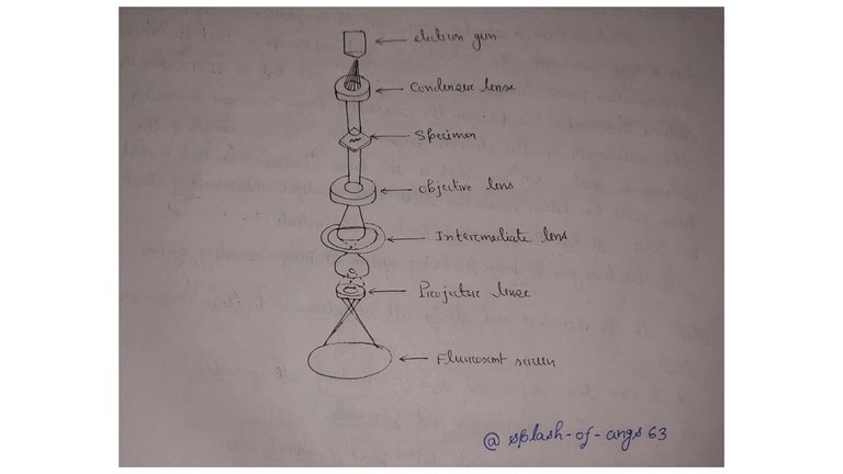
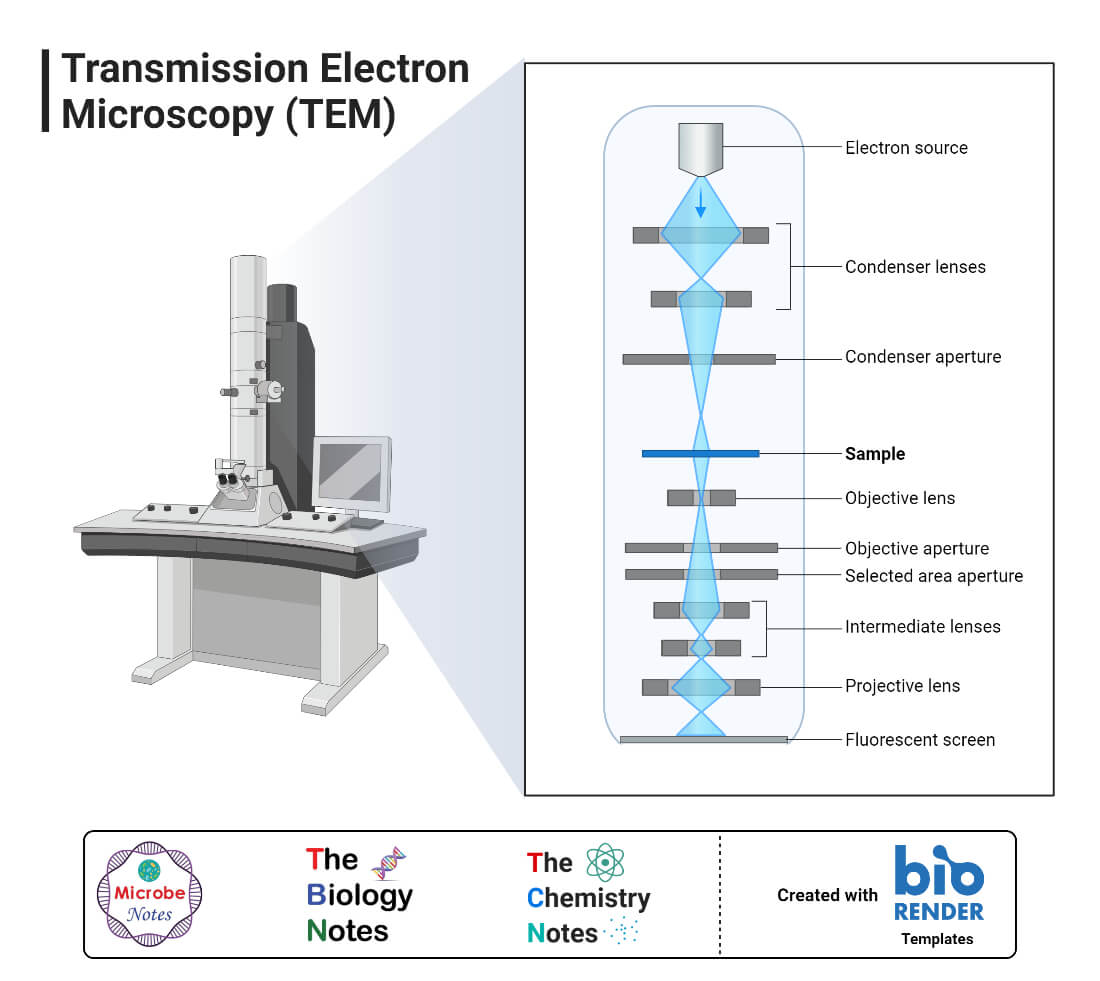
TEM has three working parts which includes
- electron gun
- image producing system
- image recording system
The function of all these are more or less similar to what we have discussed in SEM.
Some of the applications of TEM are-
- To visualise and study the cell structure of bacteria, viruses and fungi.
- To view the shapes and sizes of microbial cell organelles.
- To view bacteria flagella and plasmids
- To study and differentiate between plant and animal cells.
Modern day TEMs have enormous advantages. They have pretty high magnification power of about 2 million times than that of light microscope. The training of handling the device is not much laborious. The image produced are of very high quality with high clarity.
Transmission electron microscopy
TEM by MicrobeNotes
Review article of TEM
Transmission electron microscope-An overview by ScienceDirect
Scanning Electron Microscope: Principle and Working |ChemFam #12|
Drugs: Classification and drug-target interaction |ChemFam #11|
What are orbitals and quantum numbers? |ChemFam #10|
Quantum mechanical model of an atom |ChemFam #09|
A case study about the growth mechanism of CNT |ChemFam #08|
Carbon Nanotubes (Buckytubes): Types and Synthesis |ChemFam #07|
Nanomaterials: Classification and Approach for Synthesis |ChemFam #06|
Azadirachtin: Isolation, Extraction and Mechanism of Action |ChemFam #05|
Woodward-Fieser Rules for Calculating λmax |ChemFam #04|
Chemistry in ancient India |ChemFam #03|
How do soaps clean the dirt? |ChemFam #02|
What is anti egg white injury factor? |ChemFam #01|
PS The thumbnail image is being created by me using canva.com taking template image from MicrobeNotes

Congratulations @splash-of-angs63! You have completed the following achievement on the Hive blockchain And have been rewarded with New badge(s)
Your next target is to reach 4000 upvotes.
You can view your badges on your board and compare yourself to others in the Ranking
If you no longer want to receive notifications, reply to this comment with the word
STOPCheck out our last posts:
https://twitter.com/1028581054087553024/status/1637858524179881991
The rewards earned on this comment will go directly to the people sharing the post on Twitter as long as they are registered with @poshtoken. Sign up at https://hiveposh.com.
Thanks for your contribution to the STEMsocial community. Feel free to join us on discord to get to know the rest of us!
Please consider delegating to the @stemsocial account (85% of the curation rewards are returned).
Thanks for including @stemsocial as a beneficiary, which gives you stronger support.